EV Inductive Charger PCB Assembly Multi-Port Qi Wireless Intelligent Solar Charger PCBA

Still deciding? Get samples of $ !
Order Sample

Product Description

📊 Basic Information
Model NO.
Solar charger PCBA
Layers
Single-Layer
Base Material
Aluminium Core PCB
Customized
Customized
Service
One-Step PCB Service
Solder Mask
Blue, Green, Red, Black, White
BGA Ball Pitch
0.4mm
Surface Finishing
HASL / OSP / Immersion Gold
Copper Thickness
0.5-5oz
Board Thickness
1.6 ±0.1mm
Min Line Width
3/3mil
Production Cap.
30,000 Pieces
📦 Packaging & Delivery
Package Size
10.00cm * 10.00cm * 5.00cm
Gross Weight
1.000kg
Lead Time
10 days (1-10 Pcs); Negotiable (>10 Pcs)
📝 Product Description

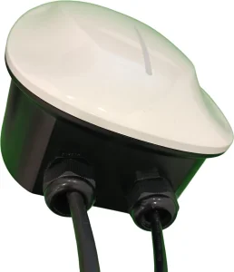
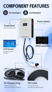
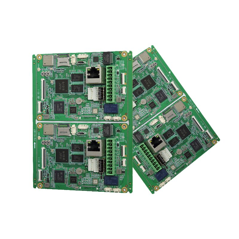
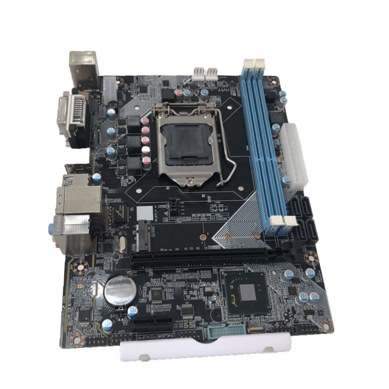
Elevate your charging solutions with our advanced Charger PCBA. This cutting-edge circuit board is meticulously crafted to meet the demands of modern devices, providing optimal power delivery and ensuring a fast and efficient charging experience.

Designed for compatibility with a wide range of devices, our Charger PCBA boasts reliability and longevity. The precision engineering behind each circuit board guarantees stable power output, protecting your devices from overcharging and other electrical issues.

Efficient Power Delivery: Faster charging times.
Universal Compatibility: Works with various devices.
Reliable Performance: Built to last and protect.
Precision Engineering: Stable power output.
📷 Product Showcase
🛠️ Technical Capabilities
Feature Item Technical Specification
Assembly TypeFR4, FPC, Rigid-flex PCB, Metal base PCB
Max Assembly SizeL510 * W460mm
Assembly Thickness0.2mm - 3.0mm
DIP Accuracy+/- 0.04mm
Minimum Pitch0.3mm
Test ServicesIQC, IPQC, SPI, AOI, X-Ray, Function Test
SMT Capacity5 million points / day
⚙️ PCB Specifications
PCB Layers1 - 24 layers
PCB MaterialsCEM1, CEM3, Rogers, FR-4, High Tg FR-4, Aluminum, Halogen Free
Max Board Size620 * 1100mm
Minimum Hole Size0.20mm
Surface FinishedHASL Lead-free, ENIG, OSP, Gold Finger, Immersion Silver
Inspection StandardIPC-A-610 CLASS II
Frequently Asked Questions
1. How do you guarantee the quality of the PCBA?
We ensure high quality through a rigorous process including a pre-production sample before mass production and a final 100% inspection before shipment using AOI and X-ray testing.
2. What types of assembly services can you provide?
We offer a one-stop solution including PCB manufacturing, component sourcing, and PCB assembly (PCBA) for various industries such as telecom, IOT, medical, and automotive.
3. What testing methods are used for BGA and complex components?
We use advanced X-Ray detection for BGA, QFN, and other precision devices to inspect hidden solder joints and ensure connection integrity.
4. What is the typical delivery time for production?
For prototypes, we can deliver within 24 hours. Small production runs typically take 72 hours, while medium-sized production orders are usually completed within 5 working days.
5. Which file formats are required for a quotation?
To provide an accurate quote and start production, we require the BOM (Bill of Materials) list and the PCB Gerber files.
6. Do you provide component sourcing services?
Yes, we provide full component procurement services, substitute material solutions for cost reduction, or we can work with core components provided by the customer.

Related Products